

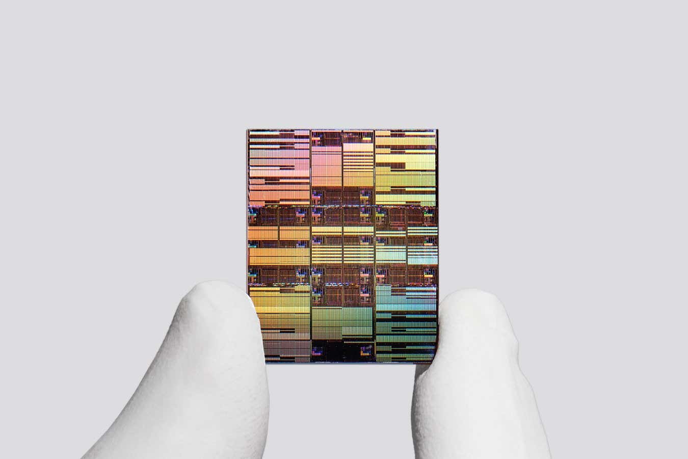
There is a new record for tiny, powerful computer chips. IBM’s prototype chip is the size of a fingernail, yet packs in almost 100 billion transistors – nearly twice as many as the previous state-of-the-art chip – thanks to a three-dimensional technique.
The company says the 10 millimetre by 15 millimetre chip will offer 70 per cent higher energy efficiency and 50 per cent higher performance than current leading chips, and will be in commercial devices within 10 years.
For decades, the name given to chip-manufacturing processes referred to the size of individual transistors in nanometres: 10 nanometres, 5 nanometres, etc. And the smaller things got, the better – smaller components tend to mean higher density and therefore faster computation for a chip of a given size, as well as lower energy use.
But in recent years, the situation has become rather more complex, says Huiming Bu at IBM. Size names have now decoupled from any physical reality and have become nothing more than marketing terms.
So while IBM refers to this latest technology as “0.7 nanometre”, it doesn’t actually claim that its components are that small, even though it packs in transistors with record density. The real innovation – which Bu says took 15 years of development – is a process to stick together two layers of silicon chips that produces all the electrical connections needed between the two, doesn’t overheat and can be mass produced.
“Our whole industry has been scaling transistors in the X-axis dimension and the Y-axis dimension for all the 60-plus years [of chip manufacturing],” says Bu. “It’s the first time we’ll enable transistor scaling in the Z direction.”
IBM wouldn’t give precise details on the dimensions of components in the new technology, but the information they did release suggests that the technology is essentially two layers of the first working 2-nanometre chip, which IBM announced in 2021. That original technology is now manufactured by many of the world’s leading chip foundries and it is expected that it will make it into the next Apple iPhone.
Because of the vast complexity and cost involved in designing and making new chips, the industry collaborates on setting out a roadmap of what new technologies need to be created and brought to market and by when, orchestrated by the not-for-profit Interuniversity Microelectronics Centre, which does much of the research and development. Though IBM’s 0.7-nanometre technology has yet to be commercially tested, it is an expected step in global chip-making that will probably be followed by other makers.
Bu hopes that, in another decade, the new 0.7-nanometre chips will be making it to commercial devices, but says the technology is increasingly having to push against the laws of physics to battle unwanted quantum effects, current leakage and other problems that arise at such minuscule scales. Parts of the latest chips are just 15 silicon atoms thick.
Owen Guy at Swansea University in the UK says other chip makers are making claims about similarly high transistor density when they are actually using multiple layers of silicon separated by thick layers of substrate, which doesn’t allow true 3D design like IBM claims, as connections can’t be easily made from one layer to the other and can be problematic to cool. “There’s a lot of smoke and mirrors about this stuff now.”
He says chip components have gotten so small now that shrinking the size of transistors – even if a chip requires billions of them – isn’t going to make a device like a laptop or smartphone smaller in practice. The push for ever-smaller components is more about extracting better energy efficiency and cooling benefits to give mobile devices a better battery life or reduce the energy consumption of data centres.
One of the main challenges now will be how to integrate IBM’s new chip technology into the global manufacturing chain and get it into devices. Chips are made in batches of hundreds on a single 300-millimetre silicon wafer that contains trillions of individual transistors, then cut into individual parts. Complex machinery performs thousands of individual operations on the wafer, setting down layers of circuit, insulation and various chemicals with thicknesses of just a few nanometres. Adding an untested new feature like IBM’s second layer won’t be simple.
Some chip makers aspire to make an even smaller “0.2-nanometre” technology, at which point parts of the circuit could be a single atom wide. “The ultimate limit is one electron and one atom.” says Guy. “It’s probably around the 2050 mark where we’re going to have to have quantum technologies to make the next big leap.”
Topics:
